
. Semiconductor process protective film
. high-end materials precision die-cutting
Our products are primarily used in wafer semiconductor manufacturing, optical panel manufacturing, and the protection of consumer electronics casings and bodies. We possess exceptional capabilities in custom material development, enabling us to collaboratively evaluate the physical properties and structure of materials according to customer specifications and stringent material characteristics. We then tailor-make exclusive processing procedures and special die-cutting structures to meet the absolute requirements of high-tech industries for dust control and high yield rates.
Die-cut products with special environmental specifications
Types of die-cut products
Special environmental control of materials
Precision Product Manufacturing Process and Packaging Instructions
Semiconductor manufacturing process-specific die-cutting technology
We combine the high cleanliness and low residue requirements of high-tech wafer fabrication consumables with an integrated molding process implemented in a Class 1000 cleanroom, precisely planning automated processes to ensure perfect integration with downstream large-scale assembly lines:
1. Die Cutting process and multiple delivery methods
We possess superior multi-stage progressive die-cut technology, enabling us to perform multiple precision die-cuts on highly complex structures to finalize multilayer film composites. Our shipping methods are highly flexible, fully compatible with our clients' mechanical assembly or automated die-cutting equipment, providing high-specification roll or sheet packaging.
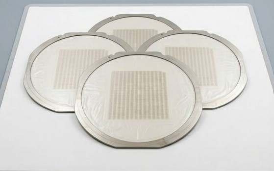
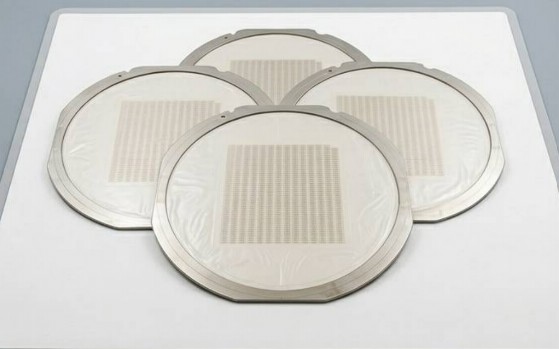
2. Semiconductor: Metal frame package
Designed specifically for semiconductor wafer cutting and packaging processes, after the die-cut material is precisely cut, we can automatically align and pre-attach the adhesive material to a standard metal frame in a cleanroom for shipment, helping customers eliminate pre-processing steps and significantly shorten the process cycle.
3. Design automated processes according to customer needs
We possess extensive experience in engineering automation design, enabling us to collaborate with R&D personnel to deeply explore processing paths and optimize feeding and die stress. We optimize production lines with the most scientific process simplification solutions, helping customers achieve accurate, fast, and high-yield high-volume continuous production targets.
Assess your semiconductor and wafer fabrication adhesive needs
Whether it's wafer consumable protective film, semiconductor DAF packaging materials, high heat-resistant PI material die-cutting, or custom-made tapes with special shapes requiring low-temperature control, we welcome your exclusive technical consultation and sample quotation.
contact